Parallel Flash memory interface is same as SRAM interface, except
that the flash memory requires a 12V/5V programming voltage
to erase and write new data.
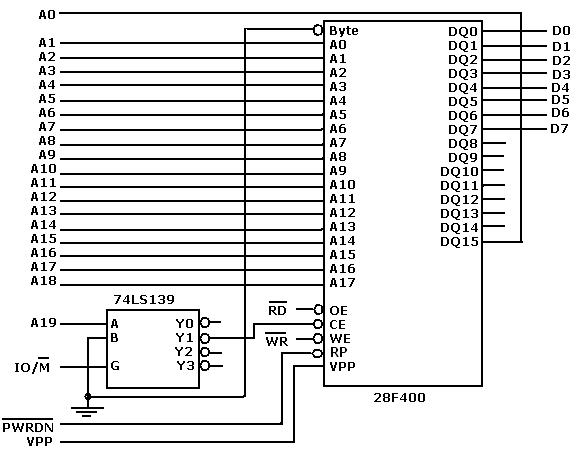
The above figure is the schematic circuit diagram of a
NOR flash IC 28F400 from Intel interfaced to a 16-bit (data)
processor or a microcontroller. The 28F400 can be configured
as 512K x 8 memory device or as a 256K x 16 memory device.
Here in the above case its 512K x 8 configuration. The control
connections pins CE, OE & WE are similar to SRAM interface.
The A0 - A17 are address pins and DQ0 to DQ15 are data pins.
The function of each control pins are,
OE (OUTPUT ENABLE): Enables the device's outputs through the data buffers during a read cycle. OE is active low.
WE (WRITE ENABLE): Controls writes to the command register and array blocks. WE is active low. Addresses and data are latched on the rising edge of the WE pulse.
CE (CHIP ENABLE): Activates the device's control logic, input buffers, decoders and sense amplifiers. CE is active low. CE high de-selects the memory device and reduces power consumption to standby levels. If CE and RP are high, but not at a CMOS high level, the standby current will increase due to current flow through the CE and RP input stages.
BYTE: Configures whether the device operates in byte-wide mode (x8) or word-wide mode (x16). This pin must be set at power-up or return from deep power-down and not changed during device operation. BYTE pin must be controlled at CMOS levels to meet the CMOS current specification in standby mode.
When BYTE is at logic low, the byte-wide mode is enabled, where data is read and programmed on DQ0-DQ7 and DQ15/A-1 becomes the lowest order address that decodes between the upper and lower byte. DQ8-DQ14 are tri-stated during the byte-wide mode.
When BYTE is at logic high, the word-wide mode is enabled, where data is read and programmed on DQ0-DQ15.
Vpp (PROGRAM/ERASE POWER SUPPLY): For erasing memory array blocks or programming data in each block, a voltage either of 5 V ± 10% or 12 V ± 5% must be applied to this pin. When VPP < VPPLK all blocks are locked and protected against Program and Erase commands.
RP/PWD (RESET/DEEP POWER-DOWN): Uses three voltage levels (VIL, VIH, and VHH) to control two different functions: reset/deep power-down mode and boot block unlocking. It is backward compatible with the BX/BL/BV products. When RP is at logic low, the device is in reset/deep power-down mode, which puts the outputs at High-Z, resets the Write State Machine, and draws minimum current.
When RP is at logic high, the device is in standard operation. When RP transitions from logic-low to logic-high, the device defaults to the read array mode.
When RP is at VHH, the boot block is unlocked and can be programmed or erased. This overrides any control from the WP input.
The decoder IC 74LS139 is employed in the above circuit for selecting the flash memory through A19 and IO/M as inputs.
Serial flash is NOR flash memory incorporating a serial interface, specifically, a serial peripheral interface (SPI) bus.


Serial flash offers advantagesin cost and miniaturization over parallel flash.
The A0 - A17 are address pins and DQ0 to DQ15 are data pins.
The function of each control pins are,
OE (OUTPUT ENABLE): Enables the device's outputs through the data buffers during a read cycle. OE is active low.
WE (WRITE ENABLE): Controls writes to the command register and array blocks. WE is active low. Addresses and data are latched on the rising edge of the WE pulse.
CE (CHIP ENABLE): Activates the device's control logic, input buffers, decoders and sense amplifiers. CE is active low. CE high de-selects the memory device and reduces power consumption to standby levels. If CE and RP are high, but not at a CMOS high level, the standby current will increase due to current flow through the CE and RP input stages.
BYTE: Configures whether the device operates in byte-wide mode (x8) or word-wide mode (x16). This pin must be set at power-up or return from deep power-down and not changed during device operation. BYTE pin must be controlled at CMOS levels to meet the CMOS current specification in standby mode.
When BYTE is at logic low, the byte-wide mode is enabled, where data is read and programmed on DQ0-DQ7 and DQ15/A-1 becomes the lowest order address that decodes between the upper and lower byte. DQ8-DQ14 are tri-stated during the byte-wide mode.
When BYTE is at logic high, the word-wide mode is enabled, where data is read and programmed on DQ0-DQ15.
Vpp (PROGRAM/ERASE POWER SUPPLY): For erasing memory array blocks or programming data in each block, a voltage either of 5 V ± 10% or 12 V ± 5% must be applied to this pin. When VPP < VPPLK all blocks are locked and protected against Program and Erase commands.
RP/PWD (RESET/DEEP POWER-DOWN): Uses three voltage levels (VIL, VIH, and VHH) to control two different functions: reset/deep power-down mode and boot block unlocking. It is backward compatible with the BX/BL/BV products. When RP is at logic low, the device is in reset/deep power-down mode, which puts the outputs at High-Z, resets the Write State Machine, and draws minimum current.
When RP is at logic high, the device is in standard operation. When RP transitions from logic-low to logic-high, the device defaults to the read array mode.
When RP is at VHH, the boot block is unlocked and can be programmed or erased. This overrides any control from the WP input.
The decoder IC 74LS139 is employed in the above circuit for selecting the flash memory through A19 and IO/M as inputs.
Serial flash is NOR flash memory incorporating a serial interface, specifically, a serial peripheral interface (SPI) bus.
Serial flash read timing diagram
Serial flash offers advantagesin cost and miniaturization over parallel flash.
Serial Flash Advantages
- Smaller, Thinner Package Development
- Wafer-level CSPs; smaller, thinner molded package USLPs
Advantage: Fewer pins enable a level of ultra-miniaturization difficult to achieve with parallel products. - Fast Data Transfer
- Eight times faster than general-purpose serial flash → Full read of 4 Mbit in only 10.5 ms.
Advantage: Fewer pins enable faster reading than in parallel flash. - Fast Writing
- High-speed rewriting, five times faster than competitive products →
High-speed rewriting, five times faster than competitive products → Full
write of 16 Mbit in only 4.5 s.
Advantage: Significantly reduces work time during writing. - Erasure on a Smaller Scale
- Compared with competitive 64 KB products, SANYO offers 256 bytes and 4 KB products.
Advantage: EEPROM replacement is possible.
No comments:
Post a Comment