Introduction to I²C and SPI protocols
Today, at the low end of the communication protocols, we find I²C (for ‘Inter-Integrated Circuit’, protocol) and SPI (for ‘Serial Peripheral Interface’). Both protocols are well-suited for communications between integrated circuits, for slow communication with on-board peripherals. At the roots of these two popular protocols we find two major companies – Philips for I²C and Motorola for SPI – and two different histories about why, when and how the protocols were created.
The I²C bus was developed in 1982; its original purpose was to provide an easy way to connect a CPU to peripherals chips in a TV set. Peripheral devices in embedded systems are often connected to the microcontroller as memory-mapped I/O devices. One common way to do this is connecting the peripherals to the microcontroller parallel address and data busses. This results in lots of wiring on the PCB (printed circuit board) and additional ‘glue logic’ to decode the address bus on which all the peripherals are connected. In order to spare microcontroller pins, additional logic and make the PCBs simpler – in order words, to lower the costs – Philips labs in Eindhoven (The Netherlands) invented the ‘Inter-Integrated Circuit’, IIC or I²C protocol that only requires 2 wires for connecting all the peripheral to a microcontroller. The original specification defined a bus speed of 100 kbps (kilo bits per second). The specification was reviewed several times, notably introducing the 400 kbps speed in 1995 and – since 1998, 3.4 Mbps for even faster peripherals.
It seems the Serial Peripheral Protocol (SPI) was first introduced with the first microcontroller deriving from the same architecture as the popular Motorola 68000 microprocessor, announced in 1979. SPI defined the external microcontroller bus, used to connect the microcontroller peripherals with 4 wires. Unlike I²C, it is hard to find a formal separate ‘specification’ of the SPI bus – for a detailed ‘official’ description, one has to read the microcontrollers data sheets and associated application notes.
SPI:
SPI is quite straightforward – it defines features any digital electronic engineer would think of if it were to quickly define a way to communicate between 2 digital devices. SPI is a protocol on 4 signal lines (please refer to figure 1):
· A clock signal named SCLK, sent from the bus master to all slaves; all the SPI signals are synchronous to this clock signal;
· A slave select signal for each slave, SSn, used to select the slave the master communicates with;
· A data line from the master to the slaves, named MOSI (Master Out-Slave In)
· A data line from the slaves to the master, named MISO (Master In-Slave Out).

SPI is a single-master communication protocol. This means that one central device initiates all the communications with the slaves. When the SPI master wishes to send data to a slave and/or request information from it, it selects slave by pulling the corresponding SS line low and it activates the clock signal at a clock frequency usable by the master and the slave. The master generates information onto MOSI line while it samples the MISO line (refer to figure 2).

Four communication modes are available (MODE 0, 1, 2, 3) – that basically define the SCLK edge on which the MOSI line toggles, the SCLK edge on which the master samples the MISO line and the SCLK signal steady level (that is the clock level, high or low, when the clock is not active). Each mode is formally defined with a pair of parameters called ‘clock polarity’ (CPOL) and ‘clock phase’ (CPHA).

A master/slave pair must use the same set of parameters – SCLK frequency, CPOL, and CPHA for a communication to be possible. If multiple slaves are used, that are fixed in different configurations, the master will have to reconfigure itself each time it needs to communicate with a different slave.
This is basically all what is defined for the SPI protocol. SPI does not define any maximum data rate, not any particular addressing scheme; it does not have a acknowledgement mechanism to confirm receipt of data and does not offer any flow control. Actually, the SPI master has no knowledge of whether a slave exists, unless ‘something’ additional is done outside the SPI protocol. For example a simple codec won’t need more than SPI, while a command-response type of control would need a higher-level protocol built on top of the SPI interface. SPI does not care about the physical interface characteristics like the I/O voltages and standard used between the devices. Initially, most SPI implementation used a non-continuous clock and byte-by-byte scheme. But many variants of the protocol now exist, that use a continuous clock signal and an arbitrary transfer length.
I²C :
I²C is a multi-master protocol that uses 2 signal lines. The two I²C signals are called ‘serial data’ (SDA) and ‘serial clock’ (SCL). There is no need of chip select (slave select) or arbitration logic. Virtually any number of slaves and any number of masters can be connected onto these 2 signal lines and communicate between each other using a protocol that defines:
· 7-bits slave addresses: each device connected to the bus has got such a unique address;
· data divided into 8-bit bytes
· a few control bits for controlling the communication start, end, direction and for an acknowledgment mechanism.
The data rate has to be chosen between 100 kbps, 400 kbps and 3.4 Mbps, respectively called standard mode, fast mode and high speed mode. Some I²C variants include 10 kbps (low speed mode) and 1 Mbps (fast mode +) as valid speeds.
Physically, the I²C bus consists of the 2 active wires SDA and SCL and a ground connection (refer to figure 4). The active wires are both bi-directional. The I2C protocol specification states that the IC that initiates a data transfer on the bus is considered the Bus Master. Consequently, at that time, all the other ICs are regarded to be Bus Slaves.

First, the master will issue a START condition. This acts as an 'Attention' signal to all of the connected devices. All ICs on the bus will listen to the bus for incoming data.
Then the master sends the ADDRESS of the device it wants to access, along with an indication whether the access is a Read or Write operation (Write in our example). Having received the address, all IC's will compare it with their own address. If it doesn't match, they simply wait until the bus is released by the stop condition (see below). If the address matches, however, the chip will produce a response called the ACKNOWLEDGE signal.
Once the master receives the acknowledge, it can start transmitting or receiving DATA. In our case, the master will transmit data. When all is done, the master will issue the STOP condition. This is a signal that states the bus has been released and that the connected ICs may expect another transmission to start any moment.
When a master wants to receive data from a slave, it proceeds the same way, but sets the RD/nWR bit at a logical one. Once the slave has acknowledged the address, it starts sending the requested data, byte by byte. After each data byte, it is up to the master to acknowledge the received data (refer to figure 5).

START and STOP are unique conditions on the bus that are closely dependent of the I²C bus physical structure. Moreover, the I²C specification states that data may only change on the SDA line if the SCL clock signal is at low level; conversely, the data on the SDA line is considered as stable when SCL is in high state (refer to figure 6 hereafter).

At the physical layer, both SCL and SDA lines are open-drain I/Os with pull-up resistors (refer to figure 4). Pulling such a line to ground is decoded as a logical zero, while releasing the line and letting it flow is a logical one. Actually, a device on a I²C bus ‘only drives zeros’.
Here we come to where I²C is truly elegant. Associating the physical layer and the protocol described above allow flawless communication between any number of devices, on just 2 physical wires.
For example, what happens if 2 devices are simultaneously trying to put information on the SDA and / or SCL lines?
At electrical level, there is actually no conflict at all if multiple devices try to put any logic level on the I²C bus lines simultaneously. If one of the drivers tries to write a logical zero and the other a logical one, then the open-drain and pull-up structure ensures that there will be no shortcut and the bus will actually see a logical zero transiting on the bus. In other words, in any conflict, a logic zero always ‘wins’.
The bus physical implementation also allows the master devices to simultaneously write and listen to the bus lines. This way, any device is able to detect collisions. In case of a conflict between two masters (one of them trying to write a zero and the other one a one), the master that gains the arbitration on the bus will even not be aware there has been a conflict: only the master that looses will know – since it intends to write a logic one and reads a logic zero. As a result, a master that looses arbitration on a I²C will stop trying to access the bus. In most cases, it will just delay its access and try the same access later.
Moreover, the I²C protocol also helps at dealing with communication problems. Any device present on the I²C listens to it permanently. Potential masters on the I²C detecting a START condition will wait until a STOP is detected to attempt a new bus access. Slaves on the I²C bus will decode the device address that follows the START condition and check if it matches theirs. All the slaves that are not addressed will wait until a STOP condition is issued before listening again to the bus. Similarly, since the I²C protocol foresees active-low acknowledge bit after each byte, the master / slave couple is able to detect their counterpart presence. Ultimately, if anything else goes wrong, this would mean that the device ‘talking on the bus’ (master or slave) would know it by simply comparing what it sends with what is seen on the bus. If a difference is detected, a STOP condition must be issued, which releases the bus.
Additionally, I²C has got some advanced features, like extended bus addressing, clock stretching and the very specific 3.4 Mbps high speed mode.
10-bits device addressing:
Any I²C device must have a built-in 7 bits address. In theory, this means that there would be only 128 different I²C devices types in the world. Practically, there are much more different I²C devices and it is a high probability that 2 devices have the same address on a I²C bus. To overcome this limitation, devices often have multiple built-in addresses that the engineer can chose by though external configuration pins on the device. The I²C specification also foresees a 10-bits addressing scheme in order to extend the range of available devices address.
Practically, this has got the following impact on the I²C protocol (refer to figure 7):
· Two address words are used for device addressing instead of one.
· The first address word MSBs are conventionally coded as “11110” so any device on the bus is aware the master sends a 10 bits device address.

Actually, there are other reserved address codes for specific types of accesses (refer to table 1). For details about them, please refer to the I²C specification.

Clock stretching:
In an I²C communication the master device determines the clock speed. The SCL signal is an explicit clock signal on which the communication synchronizes.
However, there are situations where an I²C slave is not able to co-operate with the clock speed given by the master and needs to slow down a little. This is done by a mechanism referred to as clock stretching and is made possible by the particular open-drain / pull-up structure of a I²C bus line.
An I²C slave is allowed to hold down the clock if it needs to reduce the bus speed. The master on the other hand is required to read back the clock signal after releasing it to high state and wait until the line has actually gone high.
High speed mode
Fundamentally, the use of pull-ups to set a logic one limits the maximum speed of the bus. This may be a limiting factor for many applications. This is why the 3.4 Mbps high speed mode was introduced. Prior to using this mode, the bus master must issue a specific ‘High Speed Master’ code at a lower speed mode (for example: 400 kbps Fast Mode) (refer to Table 1), which initiates a session at 3.4 Mbps. Specific I/O buffers must also be used to let the bus to shorten the signals rise time and increase the bus speed. The protocol is also somewhat adapted in such a way that no arbitration is performed during the high speed transfer. Refer to the I²C specification for more information about the high speed mode.

Master and slave:
The master can send data to a slave or receive data from a slave - slaves do not transfer data between themselves.
Multi Master
Multi master operation is a more complex use of I2C that lets you have different controlling devices on the same bus. You only need to use this mode if you have more than one microcontroller on the bus (and you want either of them to be the bus master).
Multi master operation involves arbitration of the bus (where a master has to fight to get control of the bus) and clock synchronisation (each may a use a different clock e.g. because of separate crystal clocks for each micro).
Note: Multi master is not covered in this I2C tutorial as the more common use of I2C is to use a single bus master to control peripheral devices e.g. serial memory, ADC, RTC etc.
Data and Clock
The I2C interface uses two bi-directional lines meaning that any device could drive either line. In a single master system the master device drives the clock most of the time - the master is in charge of the clock but slaves can influence it to slow it down (See Slow Peripherals below).
The two wires must be driven as open collector/drain outputs and must be pulled high using one resistor each - this implements a 'wired AND function' - any device pulling the wire low causes all devices to see a low logic value - for high logic value all devices must stop driving the wire.
Note : If you use I2C you can not put any other (non I2C) devices on the bus as both lines are used as clock at some point (generation of START and STOP bits toggles the data line). So you can not do something clever such as keeping the clock line inactive and use the data line as a button press detector (to save pins).
You will often will find devices that you realise are I2C compatible but they are labelled as using a '2 wire interface'. The manufacturer is avoiding paying royalties by not using the words 'I2C'!
There are two wires (three if you include ground!) :
I2C Turorial: Signals definition SDA : Serial Data
SCL : Serial Clock
I2C Turorial: end of signal definition I2C Tutorial : Typical SDA and SCL signals

Speed
Standard clock speeds are 100kHz and 10kHz but the standard lets you use clock speeds from zero to 100kHz and a fast mode is also available (400kHz - Fast-mode). An even higher speed (3.4MHz - High-speed mode) for more demanding applications - The mid range PIC won't be up this mode yet!
Note that the low-speed mode has been omitted (10kHz) as the standard now specifies the basic system operating from 0 to 100kHz.
Slow peripherals
A slow slave device may need to stop the bus while it gathers data or services an interrupt etc. It can do this while holding the clock line (SCL) low forcing the master into the wait state. The master must then wait until SCL is released before proceeding.
Data transfer sequence
A basic Master to slave read or write sequence for I2C follows the following order:
I2C Tutorial : I2C basic command sequence.
1. Send the START bit (S).
2. Send the slave address (ADDR).
3. Send the Read(R)-1 / Write(W)-0 bit.
4. Wait for/Send an acknowledge bit (A).
5. Send/Receive the data byte (8 bits) (DATA).
6. Expect/Send acknowledge bit (A).
7. Send the STOP bit (P).
I2C Tutorial : end of I2C basic command sequence.
Note: You can use 7 bit or 10 bit addresses.
The sequence 5 and 6 can be repeated so that a multibyte block can be read or written.
Data Transfer from master to slaveI2C Tutorial : Instruction sequence data from master to slave
A master device sends the sequence S ADDR W and then waits for an acknowledge bit (A) from the slave which the slave will only generate if its internal address matches the value sent by the master. If this happens then the master sends DATA and waits for acknowledge (A) from the slave. The master completes the byte transfer by generating a stop bit (P) (or repeated start).
Data transfer from slave to masterI2C Tutorial : Instruction sequence data from slave to master

A similar process happens when a master reads from the slave but in this case, instead of W, R is sent. After the data is transmitted from the slave to the master the master sends the acknowledge (A). If instead the master does not want any more data it must send a not-acknowledge which indicates to the slave that it should release the bus. This lets the master send the STOP or repeated START signal.
Each device you use on the I2C bus must have a unique address. For some devices e.g. serial memory you can set the lower address bits using input pins on the device others have a fixed internal address setting e.g. a real time clock DS1307. You can put several memory devices on the same IC bus by using a different address for each.
Note: The maximum number of devices is limited by the number of available addresses and by the total bus capacitance (maximum 400pF).
All I2C addresses are either 7 bits or 10 bits. The use of 10 bit addresses is rare and is not covered here. All of our modules and the common chips you will use will have 7 bit addresses. This means that you can have up to 128 devices on the I2C bus, since a 7bit number can be from 0 to 127. When sending out the 7 bit address, we still always send 8 bits. The extra bit is used to inform the slave if the master is writing to it or reading from it. If the bit is zero are master is writing to the slave. If the bit is 1 the master is reading from the slave. The 7 bit address is placed in the upper 7 bits of the byte and the Read/Write (R/W) bit is in the LSB (Least Significant Bit).
The placement of the 7 bit address in the upper 7 bits of the byte is a source of confusion for the newcomer. It means that to write to address 21, you must actually send out 42 which is 21 moved over by 1 bit. It is probably easier to think of the I2C bus addresses as 8 bit addresses, with even addresses as write only, and the odd addresses as the read address for the same device. To take our CMPS03 for example, this is at address 0xC0 ($C0). You would uses 0xC0 to write to the CMPS03 and 0xC1 to read from it. So the read/write bit just makes it an odd/even address.
General call
The general call address is a reserved address which when output by the bus master should address all devices which should respond with an acknowledge.Its value is 0000000 (7 bits) and written by the master 0000000W. If a device does not need data from the general call it does not need to respond to it.
I2C Tutorial : Reserved addresses.
0000 000 1 START byte - for slow micros without I2C h/w
0000 001 X CBUS address - a different bus protocol
0000 010 X Reserved for different bus format
0000 011 X Reserved for future purposes
0000 1XX X Hs-mode master code
1111 1XX X Reserved for future purposes
1111 0XX X 10-bit slave addressing
I2C Tutorial : End of reserved addresses.
Most of these are not that useful for PIC microcontrollers except perhaps the START byte and 10 bit addressing.
START (S) and STOP (P) bits
START (S) and STOP (P) bits are unique signals that can be generated on the bus but only by a bus master.
Reception of a START bit by an I2C slave device resets its internal bus logic. This can be done at any time so you can force a restart if anything goes wrong even in the middle of communication.
START and STOP bits are defined as rising or falling edges on the data line while the clock line is kept high.
I2C Tutorial : text definition of START and STOP signals
START condition (S)
SCL = 1, SDA falling edge
STOP condition (P)
SCL = 1, SDA rising edge
I2C Tutorial : end of text definition of START and STOP signals
The following diagram shows the above information graphically - these are the signals you would see on the I2C bus.
I2C Tutorial : end of definition of START and STOP signalsI2C Tutorial : START (S) and STOP (P) bits.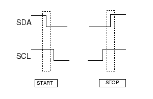
I2C Tutorial : end of definition of START and STOP signals
Note : In a single master system the only difference between a slave and a master is the master's ability to generate START and STOP bits. Both slave and master can control SDA and SCL.
Repeated START (Sr)
This seems like a confusing term at first as you ask yourself why bother with it as it is functionally identical to the sequence :
S ADDR (R/W) DATA A P
The only difference is that for a repeated start you can repeat the sequence starting from the stop bit (replacing the stop bit with another start bit).
S ADDR (R/W) DATA A Sr ADDR (R/W) DATA A P
and you can do this indefinitely.
Note: Reception of both S or Sr force any I2C device reset its internal bus logic so sending S or Sr is really resetting all the bus devices. This can be done at any time - it is a forced reset.
The main reason that the Sr bit exists is in a multi master configuration where the current bus master does not want to release its mastership. Using the repeated start keeps the bus busy so that no other master can grab the bus.
Because of this when used in a Single master configuration it is just a curiosity.
Data
All data blocks are composed of 8 bits. The initial block has 7 address bits followed by a direction bit (Read or Write). Following blocks have 8 data bits. Acknowledge bits are squeezed in between each block.
Each data byte is transmitted MSB first including the address byte.
To allow START and STOP bit generation by the master the data line (SDA) must not be changed while the clock (SCL) is high - it can only be changed when the clock is low.
Acknowledge
The acknowledge bit (generated by the receiving device) indicates to the transmitter that the the data transfer was ok. Note that the clock pulse for the acknowledge bit is always created by the bus master.
The acknowledge data bit is generated by either the master or slave depending on the data direction. For the master writing to a slave (W) the acknowledge is generated by the slave. For the master receiving (R) data from a slave the master generates the acknowledge bit.
I2C Tutorial : Definition of ACK bits
Acknowledge=0 volts
Not acknowledge=High volts
I2C Tutorial : End of definition of ACK bits
ACK data master --> slave
In this case the slave generates the acknowledge signal.
When a not-acknowledge is received by the bus master the transfer has failed and the master must generate a STOP or repeated START to abort the sequence.
ACK data slave --> master
In this case the master generates the acknowledge signal.
Normally the master will generate an acknowledge after it has received data but to indicate to the slave that no more data is required on the last byte transfer the master must generate a 'not-acknowledge'. This indicates to the slave that it should stop sending data. The master can then generate the STOP bit (or repeated START).
I²C vs SPI: is there a winner?
Let’s compare I²C and SPI on several key protocol aspects:
- Bus topology / routing / resources:
I²C needs 2 lines and that’s it, while SPI formally defines at least 4 signals and more, if you add slaves. Some unofficial SPI variants only need 3 wires, that is a SCLK, SS and a bi-directional MISO/MOSI line. Still, this implementation would require one SS line per slave. SPI requires additional work, logic and/or pins if a multi-master architecture has to be built on SPI. The only problem I²C when building a system is a limited device address space on 7 bits, overcome with the 10-bits extension.
From this point of view, I²C is a clear winner over SPI in sparing pins, board routing and how easy it is to build an I²C network.
- Throughput / Speed:
If data must be transferred at ‘high speed’, SPI is clearly the protocol of choice, over I²C. SPI is full-duplex; I²C is not. SPI does not define any speed limit; implementations often go over 10 Mbps. I²C is limited to 1Mbps in Fast Mode+ and to 3.4 Mbps in High Speed Mode - this last one requiring specific I/O buffers, not always easily available.
- Elegance:
It is often said that I²C is much more elegant than SPI, and that this last one is a very ‘rough’ (if not ‘dumb’) protocol. Actually, we tend to think the two protocols are equally elegant and comparable on robustness.
I²C is elegant because it offers very advanced features – such as automatic multi-master conflicts handling and built-in addressing management – on a very light infrastructure. It can be very complex, however and somewhat lacks performance.
SPI, on the other hand, is very easy to understand and to implement and offers a great deal of flexibility for extensions and variations. Simplicity is where the elegance of SPI lies. SPI should be considered as a good platform for building custom protocol stacks for communication between ICs. So, according to the engineer’s need, using SPI may need more work but offers increased data transfer performance and almost total freedom.
Both SPI and I2C offer good support for communication with low-speed devices, but SPI is better suited to applications in which devices transfer data streams, while I²C is better at multi master ‘register access’ application.
Used properly, the two protocols offer the same level of robustness and have been equally successful among vendors. EEPROM (Electrically-Erasable Programmable Read-Only Memory), ADC (Analog-to-Digital Converter), DAC (Digital-to-Analog Converter), RTC (Real-time clocks), microcontrollers, sensors, LCD (Liquid Crystal Display) controllers are largely available with I²C, SPI or the 2 interfaces.
This I2C tutorial shows you how the I2C protocol works at the physical bit level. It only discusses single master mode (a single controlling device) as this is the most common use for I2C in a small system.
I²C (pronounced I-squared-C) created by Philips Semiconductors and commonly written as 'I2C' stands for Inter-Integrated Circuit and allows communication of data between I2C devices over two wires. It sends information serially using one line for data (SDA) and one for clock (SCL).
Note: You can find Master mode soft I2C routines in the RTC project.
Conclusions.
In the world of communication protocols, I²C and SPI are often considered as ‘little’ communication protocols compared to Ethernet, USB, SATA, PCI-Express and others, that present throughput in the x100 megabit per second range if not gigabit per second. Though, one must not forget what each protocol is meant for. Ethernet, USB, SATA are meant for ‘outside the box communications’ and data exchanges between whole systems. When there is a need to implement a communication between integrated circuit such as a microcontroller and a set of relatively slow peripheral, there is no point at using any excessively complex protocols. There, I²C and SPI perfectly fit the bill and have become so popular that it is very likely that any embedded system engineer will use them during his/her career.
With Courtesy:
http://www.byteparadigm.com
Today, at the low end of the communication protocols, we find I²C (for ‘Inter-Integrated Circuit’, protocol) and SPI (for ‘Serial Peripheral Interface’). Both protocols are well-suited for communications between integrated circuits, for slow communication with on-board peripherals. At the roots of these two popular protocols we find two major companies – Philips for I²C and Motorola for SPI – and two different histories about why, when and how the protocols were created.
The I²C bus was developed in 1982; its original purpose was to provide an easy way to connect a CPU to peripherals chips in a TV set. Peripheral devices in embedded systems are often connected to the microcontroller as memory-mapped I/O devices. One common way to do this is connecting the peripherals to the microcontroller parallel address and data busses. This results in lots of wiring on the PCB (printed circuit board) and additional ‘glue logic’ to decode the address bus on which all the peripherals are connected. In order to spare microcontroller pins, additional logic and make the PCBs simpler – in order words, to lower the costs – Philips labs in Eindhoven (The Netherlands) invented the ‘Inter-Integrated Circuit’, IIC or I²C protocol that only requires 2 wires for connecting all the peripheral to a microcontroller. The original specification defined a bus speed of 100 kbps (kilo bits per second). The specification was reviewed several times, notably introducing the 400 kbps speed in 1995 and – since 1998, 3.4 Mbps for even faster peripherals.
It seems the Serial Peripheral Protocol (SPI) was first introduced with the first microcontroller deriving from the same architecture as the popular Motorola 68000 microprocessor, announced in 1979. SPI defined the external microcontroller bus, used to connect the microcontroller peripherals with 4 wires. Unlike I²C, it is hard to find a formal separate ‘specification’ of the SPI bus – for a detailed ‘official’ description, one has to read the microcontrollers data sheets and associated application notes.
SPI:
SPI is quite straightforward – it defines features any digital electronic engineer would think of if it were to quickly define a way to communicate between 2 digital devices. SPI is a protocol on 4 signal lines (please refer to figure 1):
· A clock signal named SCLK, sent from the bus master to all slaves; all the SPI signals are synchronous to this clock signal;
· A slave select signal for each slave, SSn, used to select the slave the master communicates with;
· A data line from the master to the slaves, named MOSI (Master Out-Slave In)
· A data line from the slaves to the master, named MISO (Master In-Slave Out).
SPI is a single-master communication protocol. This means that one central device initiates all the communications with the slaves. When the SPI master wishes to send data to a slave and/or request information from it, it selects slave by pulling the corresponding SS line low and it activates the clock signal at a clock frequency usable by the master and the slave. The master generates information onto MOSI line while it samples the MISO line (refer to figure 2).
Four communication modes are available (MODE 0, 1, 2, 3) – that basically define the SCLK edge on which the MOSI line toggles, the SCLK edge on which the master samples the MISO line and the SCLK signal steady level (that is the clock level, high or low, when the clock is not active). Each mode is formally defined with a pair of parameters called ‘clock polarity’ (CPOL) and ‘clock phase’ (CPHA).
A master/slave pair must use the same set of parameters – SCLK frequency, CPOL, and CPHA for a communication to be possible. If multiple slaves are used, that are fixed in different configurations, the master will have to reconfigure itself each time it needs to communicate with a different slave.
This is basically all what is defined for the SPI protocol. SPI does not define any maximum data rate, not any particular addressing scheme; it does not have a acknowledgement mechanism to confirm receipt of data and does not offer any flow control. Actually, the SPI master has no knowledge of whether a slave exists, unless ‘something’ additional is done outside the SPI protocol. For example a simple codec won’t need more than SPI, while a command-response type of control would need a higher-level protocol built on top of the SPI interface. SPI does not care about the physical interface characteristics like the I/O voltages and standard used between the devices. Initially, most SPI implementation used a non-continuous clock and byte-by-byte scheme. But many variants of the protocol now exist, that use a continuous clock signal and an arbitrary transfer length.
I²C :
I²C is a multi-master protocol that uses 2 signal lines. The two I²C signals are called ‘serial data’ (SDA) and ‘serial clock’ (SCL). There is no need of chip select (slave select) or arbitration logic. Virtually any number of slaves and any number of masters can be connected onto these 2 signal lines and communicate between each other using a protocol that defines:
· 7-bits slave addresses: each device connected to the bus has got such a unique address;
· data divided into 8-bit bytes
· a few control bits for controlling the communication start, end, direction and for an acknowledgment mechanism.
The data rate has to be chosen between 100 kbps, 400 kbps and 3.4 Mbps, respectively called standard mode, fast mode and high speed mode. Some I²C variants include 10 kbps (low speed mode) and 1 Mbps (fast mode +) as valid speeds.
Physically, the I²C bus consists of the 2 active wires SDA and SCL and a ground connection (refer to figure 4). The active wires are both bi-directional. The I2C protocol specification states that the IC that initiates a data transfer on the bus is considered the Bus Master. Consequently, at that time, all the other ICs are regarded to be Bus Slaves.
First, the master will issue a START condition. This acts as an 'Attention' signal to all of the connected devices. All ICs on the bus will listen to the bus for incoming data.
Then the master sends the ADDRESS of the device it wants to access, along with an indication whether the access is a Read or Write operation (Write in our example). Having received the address, all IC's will compare it with their own address. If it doesn't match, they simply wait until the bus is released by the stop condition (see below). If the address matches, however, the chip will produce a response called the ACKNOWLEDGE signal.
Once the master receives the acknowledge, it can start transmitting or receiving DATA. In our case, the master will transmit data. When all is done, the master will issue the STOP condition. This is a signal that states the bus has been released and that the connected ICs may expect another transmission to start any moment.
When a master wants to receive data from a slave, it proceeds the same way, but sets the RD/nWR bit at a logical one. Once the slave has acknowledged the address, it starts sending the requested data, byte by byte. After each data byte, it is up to the master to acknowledge the received data (refer to figure 5).
START and STOP are unique conditions on the bus that are closely dependent of the I²C bus physical structure. Moreover, the I²C specification states that data may only change on the SDA line if the SCL clock signal is at low level; conversely, the data on the SDA line is considered as stable when SCL is in high state (refer to figure 6 hereafter).
At the physical layer, both SCL and SDA lines are open-drain I/Os with pull-up resistors (refer to figure 4). Pulling such a line to ground is decoded as a logical zero, while releasing the line and letting it flow is a logical one. Actually, a device on a I²C bus ‘only drives zeros’.
Here we come to where I²C is truly elegant. Associating the physical layer and the protocol described above allow flawless communication between any number of devices, on just 2 physical wires.
For example, what happens if 2 devices are simultaneously trying to put information on the SDA and / or SCL lines?
At electrical level, there is actually no conflict at all if multiple devices try to put any logic level on the I²C bus lines simultaneously. If one of the drivers tries to write a logical zero and the other a logical one, then the open-drain and pull-up structure ensures that there will be no shortcut and the bus will actually see a logical zero transiting on the bus. In other words, in any conflict, a logic zero always ‘wins’.
The bus physical implementation also allows the master devices to simultaneously write and listen to the bus lines. This way, any device is able to detect collisions. In case of a conflict between two masters (one of them trying to write a zero and the other one a one), the master that gains the arbitration on the bus will even not be aware there has been a conflict: only the master that looses will know – since it intends to write a logic one and reads a logic zero. As a result, a master that looses arbitration on a I²C will stop trying to access the bus. In most cases, it will just delay its access and try the same access later.
Moreover, the I²C protocol also helps at dealing with communication problems. Any device present on the I²C listens to it permanently. Potential masters on the I²C detecting a START condition will wait until a STOP is detected to attempt a new bus access. Slaves on the I²C bus will decode the device address that follows the START condition and check if it matches theirs. All the slaves that are not addressed will wait until a STOP condition is issued before listening again to the bus. Similarly, since the I²C protocol foresees active-low acknowledge bit after each byte, the master / slave couple is able to detect their counterpart presence. Ultimately, if anything else goes wrong, this would mean that the device ‘talking on the bus’ (master or slave) would know it by simply comparing what it sends with what is seen on the bus. If a difference is detected, a STOP condition must be issued, which releases the bus.
Additionally, I²C has got some advanced features, like extended bus addressing, clock stretching and the very specific 3.4 Mbps high speed mode.
10-bits device addressing:
Any I²C device must have a built-in 7 bits address. In theory, this means that there would be only 128 different I²C devices types in the world. Practically, there are much more different I²C devices and it is a high probability that 2 devices have the same address on a I²C bus. To overcome this limitation, devices often have multiple built-in addresses that the engineer can chose by though external configuration pins on the device. The I²C specification also foresees a 10-bits addressing scheme in order to extend the range of available devices address.
Practically, this has got the following impact on the I²C protocol (refer to figure 7):
· Two address words are used for device addressing instead of one.
· The first address word MSBs are conventionally coded as “11110” so any device on the bus is aware the master sends a 10 bits device address.
Actually, there are other reserved address codes for specific types of accesses (refer to table 1). For details about them, please refer to the I²C specification.
Clock stretching:
In an I²C communication the master device determines the clock speed. The SCL signal is an explicit clock signal on which the communication synchronizes.
However, there are situations where an I²C slave is not able to co-operate with the clock speed given by the master and needs to slow down a little. This is done by a mechanism referred to as clock stretching and is made possible by the particular open-drain / pull-up structure of a I²C bus line.
An I²C slave is allowed to hold down the clock if it needs to reduce the bus speed. The master on the other hand is required to read back the clock signal after releasing it to high state and wait until the line has actually gone high.
High speed mode
Fundamentally, the use of pull-ups to set a logic one limits the maximum speed of the bus. This may be a limiting factor for many applications. This is why the 3.4 Mbps high speed mode was introduced. Prior to using this mode, the bus master must issue a specific ‘High Speed Master’ code at a lower speed mode (for example: 400 kbps Fast Mode) (refer to Table 1), which initiates a session at 3.4 Mbps. Specific I/O buffers must also be used to let the bus to shorten the signals rise time and increase the bus speed. The protocol is also somewhat adapted in such a way that no arbitration is performed during the high speed transfer. Refer to the I²C specification for more information about the high speed mode.
Master and slave:
The master can send data to a slave or receive data from a slave - slaves do not transfer data between themselves.
Multi Master
Multi master operation is a more complex use of I2C that lets you have different controlling devices on the same bus. You only need to use this mode if you have more than one microcontroller on the bus (and you want either of them to be the bus master).
Multi master operation involves arbitration of the bus (where a master has to fight to get control of the bus) and clock synchronisation (each may a use a different clock e.g. because of separate crystal clocks for each micro).
Note: Multi master is not covered in this I2C tutorial as the more common use of I2C is to use a single bus master to control peripheral devices e.g. serial memory, ADC, RTC etc.
Data and Clock
The I2C interface uses two bi-directional lines meaning that any device could drive either line. In a single master system the master device drives the clock most of the time - the master is in charge of the clock but slaves can influence it to slow it down (See Slow Peripherals below).
The two wires must be driven as open collector/drain outputs and must be pulled high using one resistor each - this implements a 'wired AND function' - any device pulling the wire low causes all devices to see a low logic value - for high logic value all devices must stop driving the wire.
Note : If you use I2C you can not put any other (non I2C) devices on the bus as both lines are used as clock at some point (generation of START and STOP bits toggles the data line). So you can not do something clever such as keeping the clock line inactive and use the data line as a button press detector (to save pins).
You will often will find devices that you realise are I2C compatible but they are labelled as using a '2 wire interface'. The manufacturer is avoiding paying royalties by not using the words 'I2C'!
There are two wires (three if you include ground!) :
I2C Turorial: Signals definition SDA : Serial Data
SCL : Serial Clock
I2C Turorial: end of signal definition I2C Tutorial : Typical SDA and SCL signals
Speed
Standard clock speeds are 100kHz and 10kHz but the standard lets you use clock speeds from zero to 100kHz and a fast mode is also available (400kHz - Fast-mode). An even higher speed (3.4MHz - High-speed mode) for more demanding applications - The mid range PIC won't be up this mode yet!
Note that the low-speed mode has been omitted (10kHz) as the standard now specifies the basic system operating from 0 to 100kHz.
Slow peripherals
A slow slave device may need to stop the bus while it gathers data or services an interrupt etc. It can do this while holding the clock line (SCL) low forcing the master into the wait state. The master must then wait until SCL is released before proceeding.
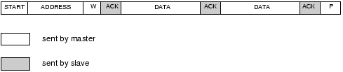
Data transfer sequence
A basic Master to slave read or write sequence for I2C follows the following order:
I2C Tutorial : I2C basic command sequence.
1. Send the START bit (S).
2. Send the slave address (ADDR).
3. Send the Read(R)-1 / Write(W)-0 bit.
4. Wait for/Send an acknowledge bit (A).
5. Send/Receive the data byte (8 bits) (DATA).
6. Expect/Send acknowledge bit (A).
7. Send the STOP bit (P).
I2C Tutorial : end of I2C basic command sequence.
Note: You can use 7 bit or 10 bit addresses.
The sequence 5 and 6 can be repeated so that a multibyte block can be read or written.
Data Transfer from master to slaveI2C Tutorial : Instruction sequence data from master to slave
A master device sends the sequence S ADDR W and then waits for an acknowledge bit (A) from the slave which the slave will only generate if its internal address matches the value sent by the master. If this happens then the master sends DATA and waits for acknowledge (A) from the slave. The master completes the byte transfer by generating a stop bit (P) (or repeated start).
Data transfer from slave to masterI2C Tutorial : Instruction sequence data from slave to master
A similar process happens when a master reads from the slave but in this case, instead of W, R is sent. After the data is transmitted from the slave to the master the master sends the acknowledge (A). If instead the master does not want any more data it must send a not-acknowledge which indicates to the slave that it should release the bus. This lets the master send the STOP or repeated START signal.
I2C Device Addressing:
Each device you use on the I2C bus must have a unique address. For some devices e.g. serial memory you can set the lower address bits using input pins on the device others have a fixed internal address setting e.g. a real time clock DS1307. You can put several memory devices on the same IC bus by using a different address for each.
Note: The maximum number of devices is limited by the number of available addresses and by the total bus capacitance (maximum 400pF).
All I2C addresses are either 7 bits or 10 bits. The use of 10 bit addresses is rare and is not covered here. All of our modules and the common chips you will use will have 7 bit addresses. This means that you can have up to 128 devices on the I2C bus, since a 7bit number can be from 0 to 127. When sending out the 7 bit address, we still always send 8 bits. The extra bit is used to inform the slave if the master is writing to it or reading from it. If the bit is zero are master is writing to the slave. If the bit is 1 the master is reading from the slave. The 7 bit address is placed in the upper 7 bits of the byte and the Read/Write (R/W) bit is in the LSB (Least Significant Bit).
The placement of the 7 bit address in the upper 7 bits of the byte is a source of confusion for the newcomer. It means that to write to address 21, you must actually send out 42 which is 21 moved over by 1 bit. It is probably easier to think of the I2C bus addresses as 8 bit addresses, with even addresses as write only, and the odd addresses as the read address for the same device. To take our CMPS03 for example, this is at address 0xC0 ($C0). You would uses 0xC0 to write to the CMPS03 and 0xC1 to read from it. So the read/write bit just makes it an odd/even address.
General call
The general call address is a reserved address which when output by the bus master should address all devices which should respond with an acknowledge.Its value is 0000000 (7 bits) and written by the master 0000000W. If a device does not need data from the general call it does not need to respond to it.
I2C Tutorial : Reserved addresses.
0000 000 1 START byte - for slow micros without I2C h/w
0000 001 X CBUS address - a different bus protocol
0000 010 X Reserved for different bus format
0000 011 X Reserved for future purposes
0000 1XX X Hs-mode master code
1111 1XX X Reserved for future purposes
1111 0XX X 10-bit slave addressing
I2C Tutorial : End of reserved addresses.
Most of these are not that useful for PIC microcontrollers except perhaps the START byte and 10 bit addressing.
START (S) and STOP (P) bits
START (S) and STOP (P) bits are unique signals that can be generated on the bus but only by a bus master.
Reception of a START bit by an I2C slave device resets its internal bus logic. This can be done at any time so you can force a restart if anything goes wrong even in the middle of communication.
START and STOP bits are defined as rising or falling edges on the data line while the clock line is kept high.
I2C Tutorial : text definition of START and STOP signals
START condition (S)
SCL = 1, SDA falling edge
STOP condition (P)
SCL = 1, SDA rising edge
I2C Tutorial : end of text definition of START and STOP signals
The following diagram shows the above information graphically - these are the signals you would see on the I2C bus.
I2C Tutorial : end of definition of START and STOP signalsI2C Tutorial : START (S) and STOP (P) bits.
I2C Tutorial : end of definition of START and STOP signals
Note : In a single master system the only difference between a slave and a master is the master's ability to generate START and STOP bits. Both slave and master can control SDA and SCL.
Repeated START (Sr)
This seems like a confusing term at first as you ask yourself why bother with it as it is functionally identical to the sequence :
S ADDR (R/W) DATA A P
The only difference is that for a repeated start you can repeat the sequence starting from the stop bit (replacing the stop bit with another start bit).
S ADDR (R/W) DATA A Sr ADDR (R/W) DATA A P
and you can do this indefinitely.
Note: Reception of both S or Sr force any I2C device reset its internal bus logic so sending S or Sr is really resetting all the bus devices. This can be done at any time - it is a forced reset.
The main reason that the Sr bit exists is in a multi master configuration where the current bus master does not want to release its mastership. Using the repeated start keeps the bus busy so that no other master can grab the bus.
Because of this when used in a Single master configuration it is just a curiosity.
Data
All data blocks are composed of 8 bits. The initial block has 7 address bits followed by a direction bit (Read or Write). Following blocks have 8 data bits. Acknowledge bits are squeezed in between each block.
Each data byte is transmitted MSB first including the address byte.
To allow START and STOP bit generation by the master the data line (SDA) must not be changed while the clock (SCL) is high - it can only be changed when the clock is low.
Acknowledge
The acknowledge bit (generated by the receiving device) indicates to the transmitter that the the data transfer was ok. Note that the clock pulse for the acknowledge bit is always created by the bus master.
The acknowledge data bit is generated by either the master or slave depending on the data direction. For the master writing to a slave (W) the acknowledge is generated by the slave. For the master receiving (R) data from a slave the master generates the acknowledge bit.
I2C Tutorial : Definition of ACK bits
Acknowledge=0 volts
Not acknowledge=High volts
I2C Tutorial : End of definition of ACK bits
ACK data master --> slave
In this case the slave generates the acknowledge signal.
When a not-acknowledge is received by the bus master the transfer has failed and the master must generate a STOP or repeated START to abort the sequence.
ACK data slave --> master
In this case the master generates the acknowledge signal.
Normally the master will generate an acknowledge after it has received data but to indicate to the slave that no more data is required on the last byte transfer the master must generate a 'not-acknowledge'. This indicates to the slave that it should stop sending data. The master can then generate the STOP bit (or repeated START).
I²C vs SPI: is there a winner?
Let’s compare I²C and SPI on several key protocol aspects:
- Bus topology / routing / resources:
I²C needs 2 lines and that’s it, while SPI formally defines at least 4 signals and more, if you add slaves. Some unofficial SPI variants only need 3 wires, that is a SCLK, SS and a bi-directional MISO/MOSI line. Still, this implementation would require one SS line per slave. SPI requires additional work, logic and/or pins if a multi-master architecture has to be built on SPI. The only problem I²C when building a system is a limited device address space on 7 bits, overcome with the 10-bits extension.
From this point of view, I²C is a clear winner over SPI in sparing pins, board routing and how easy it is to build an I²C network.
- Throughput / Speed:
If data must be transferred at ‘high speed’, SPI is clearly the protocol of choice, over I²C. SPI is full-duplex; I²C is not. SPI does not define any speed limit; implementations often go over 10 Mbps. I²C is limited to 1Mbps in Fast Mode+ and to 3.4 Mbps in High Speed Mode - this last one requiring specific I/O buffers, not always easily available.
- Elegance:
It is often said that I²C is much more elegant than SPI, and that this last one is a very ‘rough’ (if not ‘dumb’) protocol. Actually, we tend to think the two protocols are equally elegant and comparable on robustness.
I²C is elegant because it offers very advanced features – such as automatic multi-master conflicts handling and built-in addressing management – on a very light infrastructure. It can be very complex, however and somewhat lacks performance.
SPI, on the other hand, is very easy to understand and to implement and offers a great deal of flexibility for extensions and variations. Simplicity is where the elegance of SPI lies. SPI should be considered as a good platform for building custom protocol stacks for communication between ICs. So, according to the engineer’s need, using SPI may need more work but offers increased data transfer performance and almost total freedom.
Both SPI and I2C offer good support for communication with low-speed devices, but SPI is better suited to applications in which devices transfer data streams, while I²C is better at multi master ‘register access’ application.
Used properly, the two protocols offer the same level of robustness and have been equally successful among vendors. EEPROM (Electrically-Erasable Programmable Read-Only Memory), ADC (Analog-to-Digital Converter), DAC (Digital-to-Analog Converter), RTC (Real-time clocks), microcontrollers, sensors, LCD (Liquid Crystal Display) controllers are largely available with I²C, SPI or the 2 interfaces.
This I2C tutorial shows you how the I2C protocol works at the physical bit level. It only discusses single master mode (a single controlling device) as this is the most common use for I2C in a small system.
I²C (pronounced I-squared-C) created by Philips Semiconductors and commonly written as 'I2C' stands for Inter-Integrated Circuit and allows communication of data between I2C devices over two wires. It sends information serially using one line for data (SDA) and one for clock (SCL).
Note: You can find Master mode soft I2C routines in the RTC project.
Conclusions.
In the world of communication protocols, I²C and SPI are often considered as ‘little’ communication protocols compared to Ethernet, USB, SATA, PCI-Express and others, that present throughput in the x100 megabit per second range if not gigabit per second. Though, one must not forget what each protocol is meant for. Ethernet, USB, SATA are meant for ‘outside the box communications’ and data exchanges between whole systems. When there is a need to implement a communication between integrated circuit such as a microcontroller and a set of relatively slow peripheral, there is no point at using any excessively complex protocols. There, I²C and SPI perfectly fit the bill and have become so popular that it is very likely that any embedded system engineer will use them during his/her career.
With Courtesy:
http://www.byteparadigm.com
No comments:
Post a Comment